
$20-billion chip incentives with design, component focus on track for end-2025

The Union ministry of electronics and IT (Meity) has submitted the incentives proposal to the finance ministry, five people aware of the matter said, doubling the outlay for the first phase of the India Semiconductor Mission (ISM). Approval from the finance ministry is expected as early as October, after which the proposal will go to the Union Cabinet. The final clearance is likely before the close of 2025 when the first phase ends.
Meity is currently preparing a dossier that will outline the performance and returns of ISM’s first phase, and compare them with similar schemes in other countries, three people of the five people confirmed.
ISM dossier
“The finance ministry had asked for an economic projection document from Meity, seeking an understanding of how ISM’s first tranche’s returns will play out, and how India’s shaping up in comparison with other nations, especially the US, whose chip incentives are larger but market dynamics are undeniably trickier,” one of the people cited above said.
The US Chips Act provides over $52 billion in subsidies and tax credits for the semiconductor sector, while the EU’s Chips Act is mobilizing more than €43 billion in public and private investment. Other major players, including China, Japan, and South Korea, are also committing billions in direct funding, tax breaks, and grants to attract and retain key players in the industry.
Queries emailed to Meity and the finance ministry remained unanswered.
While the US Chips Act has a bigger outlay, it has been disrupted by president Donald Trump’s erratic policies, the third person said.
$10 billion package
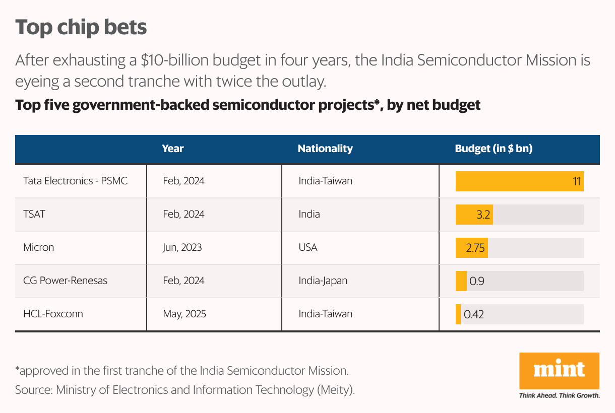
India rolled out a $10 billion package four years ago to encourage local chipmaking and related projects. During the period, the Centre has approved an $11-billion chip fab by Tata Electronics in partnership with Taiwan’s Powerchip Semiconductor Manufacturing Co., as well as testing facilities by US memory chip firm Micron, and homegrown firms such as the Murugappa group’s CG Semi and electronics manufacturer Kaynes Technology. According to Meity, the allocated funds have been nearly fully utilized.
“ISM’s net outlay may have been a fifth of America’s, but taking state and indirect incentives into account, the total expenditure from the government was easily over $15 billion. This is why Meity’s second tranche proposal is for around $20 billion, which increases incentives and reaffirms government backing,” the second person added.
Meity has focused on four key aspects for ISM 2.0, the people cited above said. These include building more sophisticated chip fabs, setting up India’s first display fab, incentivizing chip design patents, and building a robust supply chain by subsidizing components, machining, tooling and sensor suppliers to open shop in India.
“In two years, India’s second chip mission can help semiconductor startups push for indigenous chip designs catering to industrial applications, such as smart electricity metres, power grids, monitoring sensors in manufacturing, and more such use cases. India’s chip fab, which is set to produce chips ranging from 110 nanometres (nm) to 28nm in size, can build such chips within the country, giving India the kind of autonomy that it has not seen until today,” the third person added.
Design boost
As part of the new plan, the Centre may expand the design-linked incentive scheme (DLI) for semiconductors fivefold to ₹5,000 crore ($570 million) to promote chip design and patenting within the country, two of the five people cited above added. The DLI scheme helps Indian companies and startups design and develop semiconductor chips in the country.
Industry stakeholders said that such spending is necessary, and not optional, for India to maintain its momentum in the global semiconductor industry.
“Amid the current geopolitical balance, India stands a chance to offer itself as the only large and open economy for global chip firms to expand to. The US currently has an unstable environment in terms of its policies, while China is a closed economy that is more focused on building its own ventures. Right now, there are no large economies like India that would give global chip firms, including the topmost names as well, this kind of stable open markets,” said Ankush Wadhera, managing director and partner at consultancy firm, BCG India.
According to Kai Beckmann, chief executive of electronics for German chip supply chain firm Merck, while India can be among the world’s top-five countries for the semiconductor industry, its policy stability via support schemes would play a vital role. “For large firms, it’s not about financial incentives. But, government support is crucial for aspects such as policy stability, ease of doing business, and setting up a robust supply chain. That is where India’s next semiconductor scheme would come in,” he added.
Full-stack nation
Last week, at the fourth edition of Semicon India, an annual industry conference, Prime Minister Narendra Modi underlined the philosophy of India’s chip investments.
“India is now moving from back-end operations to becoming a full-stack semiconductor nation. The day is not far when India’s smallest chip will drive the world’s biggest change. Commercial chips will start being produced from this year itself, which shows how fast India is progressing in semiconductors,” he said.
“We are creating a complete ecosystem, where designing, manufacturing, packaging and high-tech devices are all available right here. Our Semiconductor Mission is not limited to just one fab or one chip manufacturing—we are creating an ecosystem that makes India self-reliant and globally competitive,” Modi added.
New horizons
On 23 August, in an interview with Mint, S. Krishnan, secretary, Meity, affirmed a similar approach.
“India does not need only chip fabs and testing plants, but also equipment suppliers, material suppliers, gases and chemicals. These are all areas that were not covered under ISM’s first plan, and need attention,” he said. Krishnan added that some components were previously covered under Meity’s Scheme for Promotion of Manufacturing of Electronic Components and Semiconductors (Specs), which has run its course.
P.N.S.V. Narasimhan, president and head of corporate affairs at homegrown tech services firm Cyient, welcomed the proposed increase in chip design incentives.
“Developing patents will take us some time. We need flexibility in sharing patents with partners, and milestone-based incentive payments should be replaced with upfront incentives. This would help us in buying strategic patents to build our own—buying such a patent from a chip foundry can cost up to $25 million,” he told Mint last week.


